

Inactive
Simplifying IT
for a complex world.
Platform partnerships
- AWS
- Google Cloud
- Microsoft
- Salesforce


A finished chip can be functionally perfect on paper and still arrive from the fab with a defect sitting in one transistor out of a billion. That single defect can be catastrophic or invisible, depending entirely on whether anyone can actually find it. This is the part of chip design nobody puts on a highlight reel. Nobody brags about their scan chains at a conference. But ask any team that has shipped silicon with a testability gap, and they’ll tell you DFT services decide more about a project’s fate than almost anything else in the flow.
DFT — design for test — exists to answer one unglamorous question: once this chip comes off the production line, how do we know which units actually work? Three techniques carry nearly all of that weight: scan, BIST, and ATPG. Together they turn “we think it works” into a number you can defend to a customer, an auditor, or a safety regulator. This is how they actually work, why skipping any one of them quietly erodes first-pass success, and what good DFT looks like on a real project.
Here’s the uncomfortable truth about manufacturing defects: they’re not rare, and they’re not optional to catch. Every wafer carries some density of physical defects — a short here, an open there, a transistor that doesn’t quite switch — and the only question is whether your test program finds them before the chip ships or after.
Catch a defect at wafer test, and the fix costs a rounding error. Let that same defect escape into a customer’s product, and the cost multiplies by a factor that gets worse the further it travels.
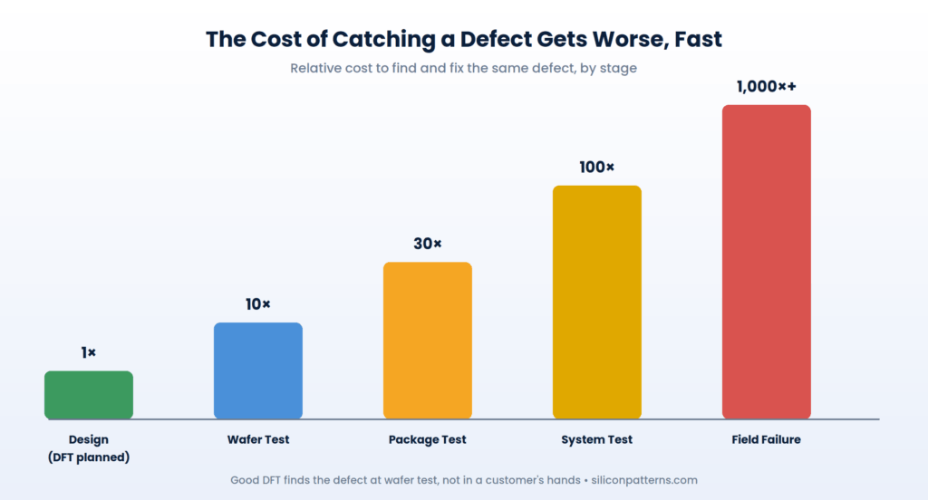
Relative cost to find and fix the same defect, by stage. Good DFT catches it early — not in a field return.
That escalating cost curve is the entire business case for DFT services. A thorough test strategy doesn’t make a chip work better. It makes sure you find out, cheaply and early, whether it actually does.
Scan, BIST, and ATPG solve three different pieces of the same puzzle. None of them alone counts as “testability” — a real DFT strategy weaves all three together.
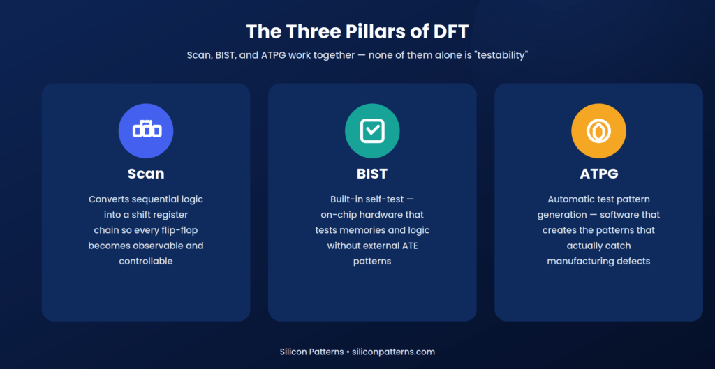
Scan gives you access. ATPG gives you patterns. BIST gives you self-sufficiency. A chip needs all three working together.
Scan converts the chip’s sequential logic into a shift register during test mode, making every flip-flop observable and controllable from just a couple of pins. ATPG (automatic test pattern generation) is the software that figures out exactly which patterns, shifted through that scan chain, will catch the defects that actually matter. BIST (built-in self-test) puts dedicated test hardware directly on the chip, letting memories and logic test themselves without an expensive external tester running every pattern.
Without scan, a chip’s internal flip-flops are nearly invisible from the outside — each one only talks to its own local logic, and probing its state means routing a signal nobody designed for.
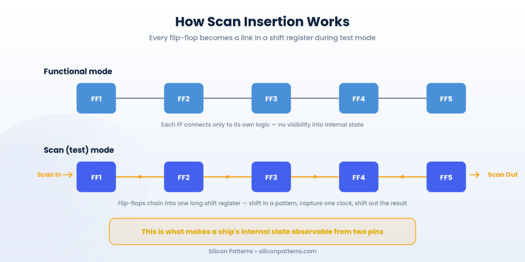
Functional mode versus scan mode. The same flip-flops, wired for a completely different job during test.
Scan insertion adds a second input and a mode-select signal to every flip-flop, then chains them together into one long shift register during test mode. Shift a test pattern in, apply a single clock pulse, shift the result out, and compare it against the expected value. Repeat that thousands of times with different patterns, and a tester can observe almost the entire internal state of a chip with millions of gates, through just a handful of pins. That single trick is what makes modern digital testing possible at all.
Once scan access exists, something still has to decide which patterns to actually run. That’s ATPG’s job, and it works through a fairly mechanical pipeline.
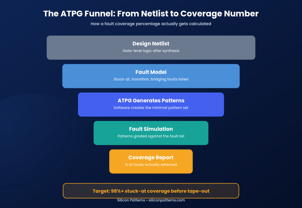
How a fault coverage percentage actually gets calculated — from gate-level netlist down to a number you can report.
ATPG software starts from the gate-level netlist and a fault model — a list of every way a manufacturing defect could realistically show up, commonly modeled as “stuck-at” faults where a signal gets stuck at 0 or 1. It generates the minimal set of patterns needed to catch each fault, then simulates those patterns against the fault list to see what actually got caught. The result is a coverage report: a percentage telling you exactly how much of the chip’s logic your test program can actually verify.
That percentage matters enormously. A chip with 85% stuck-at coverage ships with real, known gaps in its test program — faults that could sail straight through to a customer. Competent teams target 98% or higher before tape-out, and treat anything less as a flag, not a rounding error.
Scan and ATPG both assume an external tester drives the show, loading patterns and checking results. BIST flips that model. It puts the test logic on the chip itself.
Memory BIST is the most common form — dedicated hardware that runs march algorithms against every memory array on the chip, checking for stuck bits, coupling faults, and address decoder errors without ever touching an external tester. Logic BIST extends the same idea to general logic, using an on-chip pattern generator and signature compressor instead of external ATPG patterns. BIST earns its keep anywhere external test access gets expensive or impossible — in the field, during burn-in, or on a chip with so many pins committed to function that scan I/O becomes a luxury.
A DFT services engagement that’s doing its job touches far more than “add some scan chains.” A thorough scope typically includes:
Ask a prospective partner to walk through each of these explicitly. A quote that only covers scan insertion, with ATPG and BIST treated as afterthoughts, leaves real coverage gaps baked into the plan from day one.
“How much coverage is enough?” doesn’t have one universal answer. The right target depends heavily on what happens if a defective chip actually ships.
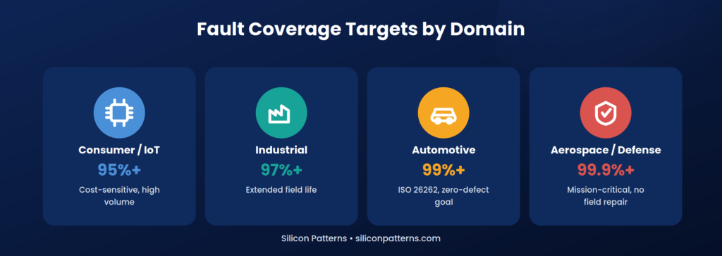
The same question — “is this chip good?” — carries very different stakes depending on where it ships.
Consumer and IoT products typically target 95% or higher, balancing cost against volume. Industrial systems push past 97%, since field life runs longer and replacement costs more. Automotive work aims for 99% or beyond, driven by ISO 26262 and a functional-safety culture that treats an undetected fault as a potential hazard rather than a nuisance. Aerospace and defense silicon pushes past 99.9%, because there’s often no field repair option at all — the part simply has to work.
Know which bracket your product falls into before a DFT budget gets set. Overshooting wastes schedule and silicon area on marginal coverage gains; undershooting ships risk nobody signed up for.
DFT doesn’t live in isolation. It threads through the entire chip design process, and treating it as a late add-on is one of the most common — and most expensive — mistakes a team can make. Scan architecture decisions made during RTL design affect synthesis. Scan chain ordering affects place-and-route congestion. ATPG pattern counts affect production test time and, directly, unit cost at volume.
This is exactly why DFT belongs inside a unified design flow rather than bolted on by a separate vendor at the end. Our semiconductor design services carry DFT planning from early RTL through sign-off as one continuous thread, not a disconnected handoff that discovers architectural conflicts after the floorplan has already locked. For programs that want every stage — architecture through DFT, physical design, and production test — owned by a single accountable team, our turnkey ASIC solutions approach removes exactly the kind of vendor seam where testability gaps tend to hide.
Scan is the hardware structure — flip-flops wired into a shift register so a tester can observe and control them. ATPG is the software that generates the test patterns run through that scan structure. BIST is self-contained on-chip test hardware that doesn’t need external patterns at all. A complete DFT strategy uses scan and ATPG together for logic, and adds BIST for memories and anywhere external test access is limited.
Typically 3–8% additional area for scan and test logic, depending on the design and the compression scheme used. That cost is almost always worth paying: the area a scan chain consumes is small next to the cost of a field failure or a full re-spin caused by an undetected defect.
It depends on the product. Consumer electronics commonly target 95%+, industrial systems 97%+, automotive 99%+ under ISO 26262, and aerospace or defense silicon 99.9%+. Set the target early, since it shapes how much DFT effort and chip area the project needs to budget.
Technically yes, but it comes at a real cost. Late DFT insertion often forces compromises in scan chain ordering and test architecture that a design planned around testability from the start would have avoided. Planning DFT alongside the architecture phase consistently produces better coverage with less area overhead than retrofitting it near tape-out.
High stuck-at coverage doesn’t guarantee every real-world defect gets caught. Modern designs increasingly add transition fault and at-speed testing to catch timing-related defects that pure stuck-at models miss entirely. A single coverage number is a strong signal, not an absolute guarantee — it’s one of several checks a mature test strategy runs.
DFT services rarely get the credit they deserve, mostly because success looks like nothing happening — no field failures, no angry customers, no emergency re-spin. Scan gives a tester access. ATPG decides what to look for. BIST lets the chip police itself. Skip or underfund any one of the three, and first-pass silicon success turns into a dice roll instead of an engineering outcome.
If you’re planning a tape-out and want DFT built into the flow from day one rather than bolted on at the end, explore our semiconductor design services, or talk to us about a fully turnkey ASIC program where testability is part of the architecture conversation from the very first meeting.

From ASIC architecture to GDSII tape-out — talk to our engineering team today.
Let’s Build Your Next Chip Together.