


Inactive
Simplifying IT
for a complex world.
Platform partnerships
- AWS
- Google Cloud
- Microsoft
- Salesforce
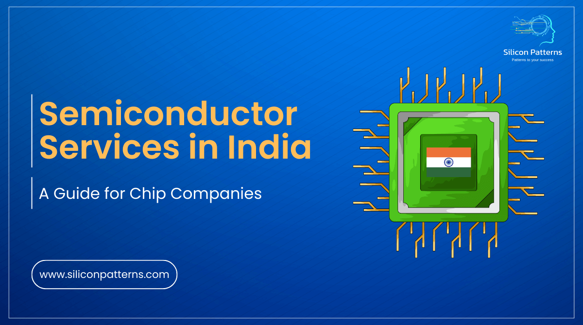
Global technology companies are increasingly relying on semiconductor services in India to accelerate chip development and reduce design complexity. With strong expertise in ASIC design, VLSI engineering, and verification technologies, India has become a major hub for semiconductor innovation. Today, semiconductor services in India support global chip companies developing processors for AI, automotive electronics, wireless communication, and high-performance computing.
As global chip companies look for innovation, scalability, and cost-effective engineering, semiconductor services in India have become an important part of the global chip development ecosystem.
India has emerged as a major semiconductor design hub, offering highly skilled engineers, strong technical expertise, and a mature semiconductor ecosystem that supports end-to-end chip design.
In this guide, we explore the key semiconductor services available in India, how they support the global chip industry, and why many companies partner with engineering teams in India for advanced semiconductor design.

The semiconductor industry continues to expand rapidly as demand for intelligent devices and connected technologies increases worldwide.
According to the Semiconductor Industry Association the global semiconductor market continues to grow due to innovation in artificial intelligence, automotive electronics, data centers, and advanced computing systems.
India has become a critical part of this ecosystem by providing highly skilled semiconductor engineers and advanced chip design capabilities.
Several factors contribute to this growth:
Semiconductor design involves multiple engineering stages, from architecture to final silicon validation. Many engineering organizations in India provide specialized expertise across the entire chip design flow.
Below are some of the most common semiconductor services available.
Application-Specific Integrated Circuit (ASIC) design is a core part of semiconductor product development.
ASIC design services in India typically include:
ASIC development requires strong expertise in hardware architecture and digital design methodologies, and many engineering teams in India support global semiconductor programs across industries such as automotive, wireless, networking, and AI accelerators.
Very Large Scale Integration (VLSI) design is the foundation of modern semiconductor engineering.
VLSI design services in India include:
India has developed a strong reputation in VLSI engineering services, with engineers contributing to complex chip designs used in high-performance computing, telecommunications, and consumer electronics.
Verification is one of the most critical phases of semiconductor development. Ensuring that the chip design behaves exactly as intended before fabrication is essential for avoiding costly silicon re-spins.
Design verification services include:
Engineering teams specializing in design verification services in India support complex SoC verification for advanced nodes and multi-billion transistor designs.
Once RTL design is verified, the chip moves into the physical design stage, where logical circuits are converted into a physical layout suitable for fabrication.
Physical design services include:
Modern semiconductor chips are fabricated using advanced process nodes developed by major semiconductor foundries such as TSMC.
Even after fabrication, semiconductor devices must undergo extensive validation to ensure functionality, performance, and reliability.
Post-silicon validation services include:
These services help ensure that semiconductor products operate correctly in real-world environments.
Many global semiconductor companies collaborate with engineering teams in India for several reasons.
India produces thousands of semiconductor and electronics engineers every year, many specializing in VLSI design, embedded systems, and chip architecture.
Engineering teams in India have experience working with advanced technologies including:
This expertise allows companies to develop complex SoC architectures for modern applications.
Semiconductor services providers in India frequently work with global design teams across the United States, Europe, and Asia, enabling round-the-clock development cycles and faster project execution.
Semiconductor design services in India support a wide range of industries, including:
As chip complexity continues to increase, companies are increasingly partnering with engineering experts to accelerate product development.
The global semiconductor industry continues to push the boundaries of innovation, driving demand for advanced engineering expertise across the entire chip design lifecycle.
With its deep talent pool, strong VLSI ecosystem, and growing semiconductor infrastructure, India has established itself as a major hub for semiconductor design and engineering services. From ASIC development and design verification to physical design and silicon validation, semiconductor services in India support the creation of next-generation chips used across multiple industries.
For global chip companies seeking reliable engineering expertise and scalable design capabilities, partnering with experienced semiconductor engineering teams can accelerate development timelines and improve design efficiency.
At Silicon Patterns, we are committed to delivering advanced semiconductor engineering solutions that support the evolving needs of the global semiconductor industry. Our team brings deep expertise across design verification, physical design, VLSI engineering, and silicon validation, enabling us to contribute to complex semiconductor programs with precision and innovation.
As the semiconductor landscape continues to evolve, collaboration between global chip companies and engineering experts will remain key to building the next generation of semiconductor technologies.

From ASIC architecture to GDSII tape-out — talk to our engineering team today.
Let’s Build Your Next Chip Together.