

Inactive
Simplifying IT
for a complex world.
Platform partnerships
- AWS
- Google Cloud
- Microsoft
- Salesforce

The first question almost every founder asks us is the one we can’t answer in a single number: “What will a custom chip cost me?”
It’s a fair question. It’s also a little like asking what a building costs. A parking garage and a hospital are both “buildings,” but nobody would quote them the same way. A custom ASIC on a mature 130nm node and a bleeding-edge 5nm AI accelerator are both “chips” — and they can differ in cost by a factor of fifty.
So instead of a number, this guide gives you the whole picture: what drives custom ASIC design cost, how long the journey really takes from idea to working silicon, and what happens at each stage. These are the honest ranges and timelines we walk our own clients through before a single line of RTL is written. If you’re deciding whether custom silicon makes sense for your product, this is the groundwork.
An ASIC — Application-Specific Integrated Circuit — is a chip built for one purpose rather than general-purpose computing. Custom ASIC design is the end-to-end engineering effort that turns your product requirement into a manufacturable chip: architecture, RTL coding, verification, physical design, and tape-out to a foundry.
The word “custom” is doing real work here. You’re not configuring an off-the-shelf part — you’re defining the silicon from the transistor budget up. That’s what unlocks an ASIC’s advantages: the lowest possible power, the smallest die, and the best performance-per-dollar once you’re shipping in volume. It’s also why the upfront investment is significant, and why getting the process right matters so much.
If you want the deeper engineering walkthrough of each design stage, we’ve written that separately in our ASIC design services guide. This article stays focused on the three questions that decide whether a project is viable: cost, timeline, and process.
Let’s start where everyone wants to start. The single biggest cost driver isn’t your design complexity — it’s the process node you choose. Mask sets alone go from tens of thousands of dollars at mature nodes to well over ten million at the leading edge.
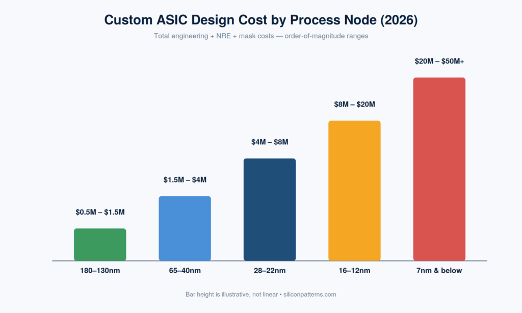
Here’s how the ranges break down, engineering plus NRE plus masks:
A word of hard-won advice: the newest node is rarely the right node. We’ve watched well-funded teams burn half their budget chasing 5nm for a product that would have shipped beautifully on 28nm. Choose the node your product needs, not the one that sounds impressive in a pitch deck.
Once you’re inside a project, the cost isn’t evenly spread. This surprises first-time chip buyers more than anything else: writing the RTL — the part people think of as “designing the chip” — is a minority of the effort.
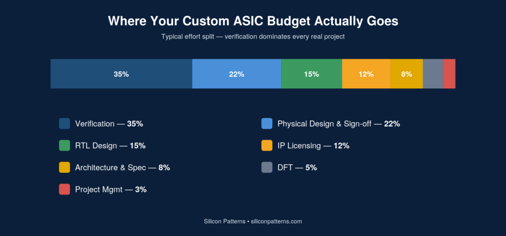
Verification routinely consumes the largest slice, often a third of the entire budget, because proving a chip works across every scenario is far harder than making it work once. When a partner’s quote shows verification as a rounding error, that’s not efficiency — that’s a re-spin waiting to happen, and a re-spin can cost more than the entire original design.
For a mid-complexity custom ASIC, plan for 16 to 18 months from kickoff to working silicon in hand. Simple derivatives on mature nodes can land in 8–10 months; large advanced-node designs can stretch past two years.
The reason it’s not faster is that the stages overlap and interlock — and one stage in particular runs almost the entire length of the project.
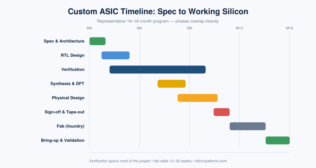
A few realities the timeline makes visible:
The single most expensive thing that can happen to your timeline is a re-spin — discovering a fatal bug after fabrication and having to fix, re-verify, and re-fab. It adds months and millions. Everything in a disciplined process exists to prevent it.
Underneath the cost and schedule sits a process that’s remarkably consistent across the industry. Six stages, each feeding the next.
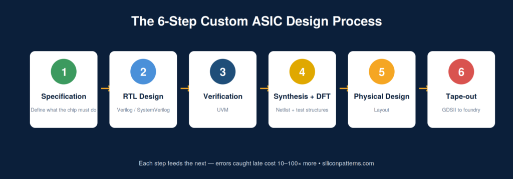
1. Specification & Architecture. The cheapest place to fix a mistake and the most expensive place to make one. Here you decide throughput, node, and what you’ll build versus license as IP. An afternoon’s decision here can save — or cost — a million dollars later.
2. RTL Design. Your architecture becomes hardware, written in Verilog or SystemVerilog. Good RTL is written with every downstream stage in mind: clean clock domains, sane resets, predictable synthesis.
3. Verification. The make-or-break stage. Using UVM and coverage-driven methodology, engineers hammer the design with scenarios no human would write by hand, measuring “done” as a coverage number rather than a gut feeling.
4. Synthesis & DFT. RTL is translated into a gate-level netlist, and design-for-test structures (scan, BIST, ATPG) are inserted so every manufactured chip can be screened for defects. Skip DFT and you get chips you can’t economically test.
5. Physical Design. The netlist becomes physical geometry — floorplanning, placement, clock trees, routing, and the long grind of timing closure across every corner. This is where power, performance, and area are won or lost.
6. Tape-out. After exhaustive sign-off checks, the final GDSII layout goes to the foundry. There’s no patching silicon after this point, which is exactly why the previous five stages are treated with such discipline.
Curious about specific stages in more depth? Our VLSI and semiconductor engineering blog breaks down verification methodology, timing closure, low-power techniques, and more in dedicated articles.
Before you spend a rupee or a dollar on custom silicon, answer one question honestly: how many units will you ship?
This is where the ASIC-versus-FPGA decision lives, and it comes down to a simple trade-off. An FPGA has almost no upfront cost but a high per-unit price. A custom ASIC has a large upfront cost but a tiny per-unit price at volume. Plot both and they cross.
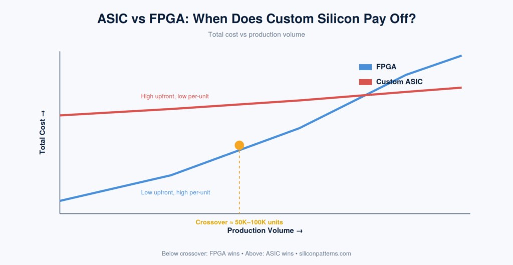
As a rough rule, the crossover sits somewhere around 50,000–100,000 units, though it shifts with complexity and node. Below that, an FPGA is usually the smarter money. Above it, a custom ASIC’s per-unit savings quickly repay the NRE — and keep paying. Many teams do both: prototype and ship early volume on FPGA, then move to a custom ASIC once demand is proven.
After years of these projects, the levers that actually matter aren’t the ones people expect:
The throughline is simple: one clean tape-out beats two cheap ones, every time.
How much does custom ASIC design cost for a startup? For most startups on mature or mainstream nodes (65nm–28nm), realistic budgets run from about $1.5M to $8M all-in, dominated by verification scope and IP licensing. Advanced nodes cost far more and rarely make sense until volume is proven.
How long does a custom ASIC take to design? Typically 16–18 months from kickoff to working silicon for a mid-complexity chip, including roughly 12–20 weeks of fabrication time that can’t be shortened.
What’s the difference between an ASIC and an SoC? An SoC (system on chip) is a type of complex ASIC that integrates many subsystems — CPU, memory, I/O, accelerators — onto one die. All SoCs are ASICs; not all ASICs are full SoCs. We cover the SoC-specific decisions in a separate guide on choosing an engineering partner.
Can I reduce cost by using an older process node? Very often, yes — and it’s the single most effective cost lever available. Mature nodes carry dramatically lower mask and NRE costs, and for many analog, industrial, and IoT products they meet every requirement.
What causes a re-spin, and how do I avoid it? A re-spin happens when a fatal bug is found after fabrication. The prevention is discipline: thorough verification, gate-level simulation, and rigorous sign-off before tape-out. It’s why cutting verification to save money is a false economy.
Custom ASIC design isn’t cheap and it isn’t fast — but for the right product at the right volume, nothing else delivers the same power, cost, and performance. The projects that succeed are the ones that respect three truths from day one: choose the node your product actually needs, treat verification as the heart of the budget rather than an afterthought, and plan for the full 16-to-18-month journey including the parts you can’t rush.
If you’re weighing a custom chip and want an honest read on what it would cost, how long it would take, and whether it’s even the right call for your volume, explore our semiconductor design services — or send us your requirement, however early, and we’ll give you a straight answer.

From ASIC architecture to GDSII tape-out — talk to our engineering team today.
Let’s Build Your Next Chip Together.