

Inactive
Simplifying IT
for a complex world.
Platform partnerships
- AWS
- Google Cloud
- Microsoft
- Salesforce

Here’s a number that surprises most first-time chip buyers: on a typical project, writing the actual design — the RTL — takes maybe 20% of the effort. The other 80% goes into everything around it. Verification. Timing closure. DFT. Sign-off. The unglamorous work that decides whether your silicon comes back working or comes back as a very expensive coaster.
That gap between “we designed a chip” and “we shipped a chip that works” is exactly what ASIC design services exist to close.
This guide walks through the full journey — specification to tape-out — the way we actually run it at Silicon Patterns, not the way it looks in a textbook flowchart. If you’re a startup building your first custom chip, or an established company deciding whether to outsource part of your silicon program, by the end you should know what happens at each stage, where projects usually go wrong, and what questions to ask before you sign with any partner.
An ASIC (Application-Specific Integrated Circuit) is a chip built to do one job extremely well — unlike an off-the-shelf processor that does many jobs adequately. Think of the difference between a tailored suit and something off the rack. The tailored version costs more upfront, but it fits your exact workload: lower power, smaller footprint, better performance per dollar at volume.
ASIC design services are the engineering muscle behind that tailoring. A services partner takes your product idea — sometimes a detailed spec, sometimes two slides and a lot of ambition — and carries it through architecture, RTL design, verification, physical design, and finally tape-out, the point where the finished layout database (GDSII) is handed to a foundry for fabrication.
Some clients hand over the entire program. Others bring us in for one stage — usually verification, because that’s where teams drown first. Both models work. What doesn’t work is discovering at month nine that nobody owns the sign-off checklist.
ASIC design sits inside the broader discipline of semiconductor design services, which also covers SoC integration, FPGA work, and embedded software — worth understanding if your product needs more than the chip itself.
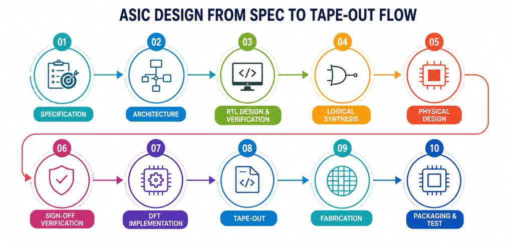
Every team draws this flow slightly differently. Below is the version that maps to how work actually gets scheduled and staffed.
This is the cheapest place to fix a mistake and the most expensive place to skip one. A change that costs an afternoon here costs a re-spin — often ₹4–8 crore ($500K–$1M+) at advanced nodes — if it’s found after fabrication.
Good architecture work answers hard questions early. What throughput does the datapath actually need — not the marketing number, the real one? Which blocks do we design fresh and which do we license as IP? What process node makes sense? In 2026, plenty of excellent products still ship on 28nm and 40nm; chasing 5nm because it sounds modern is one of the fastest ways to burn a budget.
The deliverable is a microarchitecture spec detailed enough that an engineer who’s never met you can implement from it. If a services partner rushes past this stage, that tells you something.
RTL — register-transfer level code written in Verilog or SystemVerilog — is where the architecture becomes hardware description. Experienced RTL designers write with the downstream stages in mind: clean clock domain crossings, reset strategies that won’t haunt physical design, and coding styles that synthesize predictably.
One habit we enforce internally: every block gets a lint and CDC check before it’s ever called “done.” A clock domain crossing bug is nearly invisible in simulation and catastrophic in silicon. We once traced a field failure on an inherited design to a single unsynchronized signal that misbehaved roughly once in a few billion cycles. Cheap to prevent. Brutal to debug after the fact.
This is the stage that decides your project’s fate, and it’s why verification engineers outnumber designers on most healthy teams. The industry-standard approach is UVM (Universal Verification Methodology): constrained-random testbenches that hammer the design with scenarios no human would think to write by hand, measured against functional coverage goals so “we tested it” becomes a number, not a feeling.
Modern verification also layers in formal property checking for control logic, gate-level simulation after synthesis, and — increasingly in 2026 — FPGA prototyping or emulation to run real software on the design before tape-out. If your chip will run firmware, seeing that firmware boot pre-silicon is worth every rupee.
What should you ask a partner here? Simple: “Show me a coverage report from a past project.” Teams that live coverage-driven verification will have one instantly. Teams that don’t will change the subject.
Synthesis translates RTL into a gate-level netlist mapped to the foundry’s standard cell library. Alongside it comes DFT — design for testability — where scan chains, BIST, and ATPG patterns are inserted so every chip coming off the production line can be screened for manufacturing defects.
DFT gets treated as an afterthought by inexperienced teams, and it shows: chips that can’t be tested economically, or worse, defective parts escaping to customers. Target numbers to expect from a competent partner: 98%+ stuck-at fault coverage, with a clear plan for at-speed testing.
Now the netlist becomes geometry. Floorplanning, placement, clock tree synthesis, routing, and the long grind of timing closure — coaxing every path in the design to meet its timing budget across process, voltage, and temperature corners.
This stage is where PPA (power, performance, area) is won or lost, and it’s deeply node-dependent. What works at 40nm fails at 7nm, where effects like IR drop and electromigration dominate. It’s also where an experienced team earns its fee: timing closure on a congested design is as much judgment as tooling, and no EDA license substitutes for someone who’s closed twenty designs before yours.
The final gauntlet: static timing analysis across all corners, power integrity analysis, physical verification (DRC/LVS against foundry rules), and formal equivalence checking to prove the final netlist still matches the verified RTL. Only when every check is clean does the GDSII go to the foundry.
Tape-out day is genuinely emotional. There’s no “patch it later” in silicon — the discipline of the previous fifteen months either holds or it doesn’t. Then comes the quiet 12–20 week wait for first silicon, followed by bring-up and post-silicon validation in the lab.
Anyone quoting a single number without asking about your node and complexity is guessing. But rough 2026 ranges, engineering plus NRE:
The honest lever for controlling cost isn’t rate cards — it’s avoiding re-spins. One clean tape-out beats two cheap ones, every time. This is also where working with a services team in India shifts the economics meaningfully: the same coverage-driven rigor at a cost structure that lets earlier-stage companies afford proper verification
After years on both sides of these engagements, here’s the shortlist test we’d apply to anyone — including ourselves:
How long does an ASIC project take from spec to tape-out? Twelve to eighteen months is typical for a mid-complexity SoC. Simple derivatives on mature nodes can land in 8–10 months; large advanced-node designs can run past two years.
Is an ASIC worth it versus an FPGA? FPGAs win for low volume and evolving requirements. ASICs win when volumes climb — typically past 50K–100K units — or when power and unit cost targets are non-negotiable. Many teams prototype on FPGA and graduate to ASIC.
Can I outsource just one stage, like verification? Yes, and it’s the most common entry point. Verification is a well-bounded engagement with measurable outcomes (coverage closure), which makes it a low-risk way to evaluate a partner before trusting them with a full program.
What does “tape-out” actually mean? It’s the milestone where the final, fully verified GDSII layout database is released to the foundry for mask-making and fabrication. The name is a relic from when designs were literally shipped on magnetic tape.
A successful ASIC isn’t the product of one brilliant stage — it’s the compounding of discipline across all six: a spec people actually argue over, RTL written for the flow, verification measured in coverage rather than confidence, and sign-off treated as sacred. That’s the difference between first-pass silicon and a very expensive lesson.
If you’re weighing a custom chip program in 2026 and want a partner who’s lived every stage of this flow, explore our full range of semiconductor design services — or bring us your spec, however rough, and we’ll tell you honestly what it will take to turn it into working silicon.

From ASIC architecture to GDSII tape-out — talk to our engineering team today.
Let’s Build Your Next Chip Together.