


Inactive
Simplifying IT
for a complex world.
Platform partnerships
- AWS
- Google Cloud
- Microsoft
- Salesforce
Explore the latest physical design trends for AI accelerators, including advanced node scaling, 3D ICs, chiplets, and power optimization strategies.
Artificial Intelligence is no longer confined to research labs. From hyperscale data centers to edge inference devices, AI accelerators are redefining compute infrastructure.
According to industry reports from the Semiconductor Industry Association, global semiconductor demand continues to surge due to AI-driven compute requirements.
This rapid expansion is pushing silicon engineering teams to rethink physical implementation methodologies at advanced process nodes. While architectural innovation drives algorithmic efficiency, it is the backend physical design that ultimately determines performance, power, area (PPA), and silicon reliability.
AI accelerators demand extreme transistor density and high-frequency operation. Foundries such as TSMC continue advancing 3nm and 2nm technologies, enabling higher performance per watt.
However, advanced-node physical design introduces:
Advanced node physical design for AI chips now requires:
Backend teams must integrate manufacturability awareness from day one.cialized engineering discipline requiring deep tool expertise and architectural awareness.
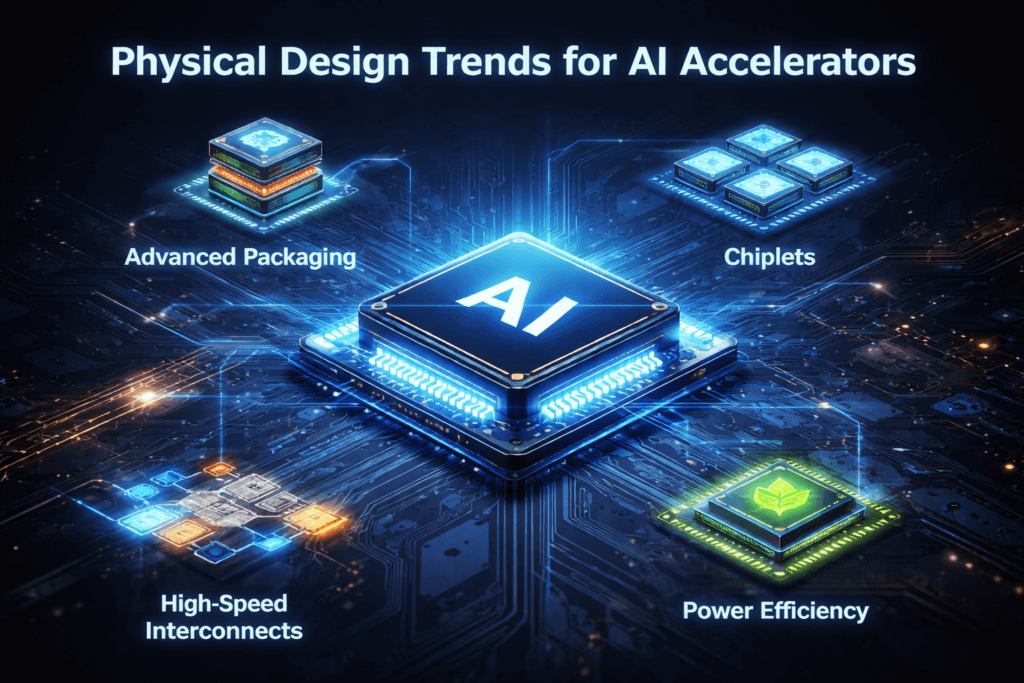
Monolithic scaling is no longer always cost-effective. The industry is rapidly transitioning toward chiplet-based AI accelerator design.
Instead of one massive die, AI accelerators are now built using multiple smaller dies connected through:
This shift impacts physical design in several ways:
AI accelerators operate under massive switching activity due to matrix multiplications and tensor operations. This creates:
Low power physical design techniques for AI accelerators now include:
Power integrity simulation is no longer a sign-off step — it is integrated throughout the design flow.
Memory bandwidth is the bottleneck of AI computation. Integration of HBM stacks changes backend implementation dramatically.
Key physical design considerations:
AI SoC backend design challenges increasingly revolve around memory-to-compute proximity optimization.
AI accelerators contain:
Without intelligent floorplanning, routing congestion can destroy timing closure.
Modern approaches include:
Interestingly, AI is now being used to design better AI hardware.
3D IC integration in AI hardware is unlocking new levels of performance per watt.
Advantages include:
However, it also introduces:
Recent technical publications available on IEEE Xplore highlight how advanced placement algorithms and ML-assisted routing are improving multi-die integration efficiency.
Physical verification for AI hardware must now include thermal-aware analysis, mechanical stress checks, and multi-die DRC validation.
One of the most exciting trends is the integration of AI within EDA tools themselves.
AI-driven backend optimization enables:
High-performance ASIC physical implementation cycles are being shortened significantly using intelligent automation.
AI accelerators often run 24/7 in data centers. Long-term reliability is critical.
Physical design teams must address:
Reliability-aware physical implementation ensures silicon longevity in high-performance AI deployments.
Physical design trends for AI accelerators are redefining what is possible in silicon engineering. From advanced node scaling and chiplet integration to AI-assisted automation and 3D IC stacking, backend implementation has become the performance backbone of modern AI systems.
As AI workloads grow more demanding, success will depend not only on architecture innovation but also on meticulous physical implementation, power integrity planning, and reliability-driven design methodologies.
At Silicon Patterns, we specialize in advanced ASIC and SoC physical design services tailored for next-generation AI accelerators. Our expertise in advanced node implementation, low-power design optimization, congestion-driven floorplanning, and sign-off closure enables clients to transform complex AI architectures into production-ready silicon.
If you are building high-performance AI hardware and need precision-driven backend execution, Silicon Patterns is ready to partner with you in shaping the future of intelligent silicon.

From ASIC architecture to GDSII tape-out — talk to our engineering team today.
Let’s Build Your Next Chip Together.