
Inactive
Simplifying IT
for a complex world.
Platform partnerships
- AWS
- Google Cloud
- Microsoft
- Salesforce
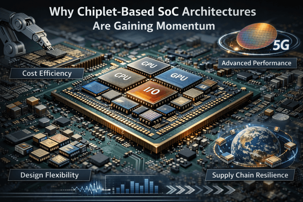
The semiconductor industry is undergoing a fundamental transformation. As traditional monolithic chip designs struggle to keep pace with rising complexity and manufacturing costs, Chiplet-Based SoC Architectures are emerging as the next major innovation in system-on-chip (SoC) design.
By breaking large chips into smaller, modular components known as chiplets, manufacturers can improve yield, reduce costs, and enhance performance scalability. This architectural shift is shaping the future of AI processors, data centers, automotive electronics, and high-performance computing platforms.
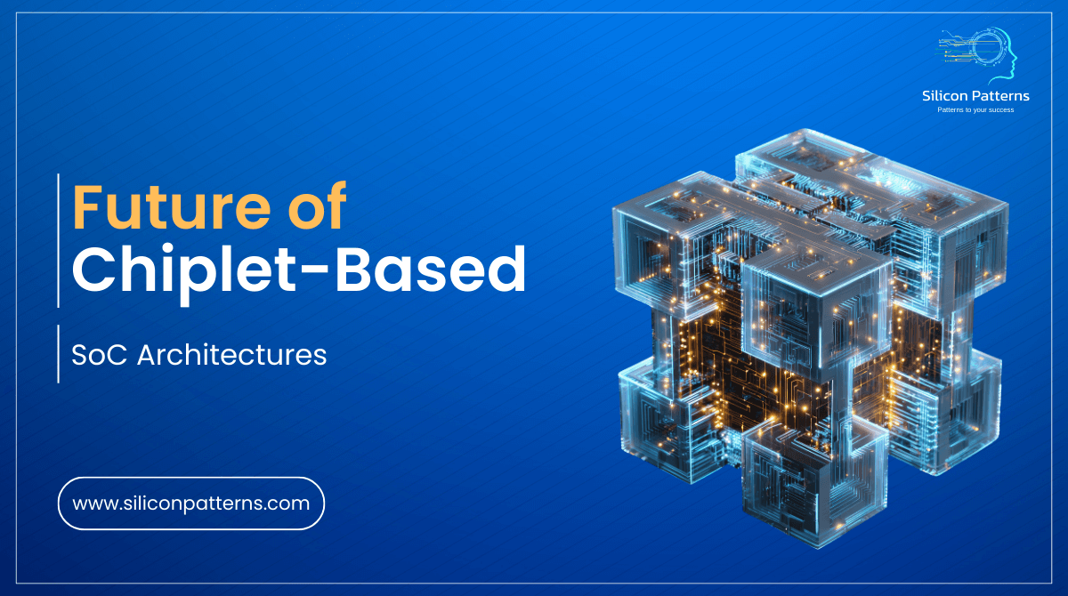
In this article, we explore the future of Chiplet-Based SoC Architectures, their benefits, challenges, and impact on next-generation semiconductor development.
Chiplet-Based SoC Architectures refer to a design methodology where multiple small functional dies (chiplets) are interconnected within a single package to function as one integrated system.
Instead of building one large monolithic die, designers separate components such as:
These chiplets communicate through high-speed interconnect technologies like silicon interposers, advanced packaging, and die-to-die interfaces.
This modular approach provides flexibility, reusability, and faster product development cycles.
Smaller chiplets are easier to manufacture with fewer defects. This leads to higher overall yield compared to large monolithic chips, reducing production waste and improving cost efficiency.
Advanced nodes are expensive. With Chiplet-Based SoC Architectures, only performance-critical blocks need to be fabricated on cutting-edge process nodes, while other components can use mature technologies.
Reusable chiplets allow semiconductor companies to design new products faster by mixing and matching validated components.
Chiplet designs enable scalable performance by adding or removing functional blocks, making them ideal for data centers, AI workloads, and customized enterprise solutions.
The success of Chiplet-Based SoC Architectures depends heavily on packaging innovations, including:
These techniques enable high bandwidth and low-latency chiplet communication.
Industry standards are playing a crucial role in enabling chiplet interoperability. Popular interfaces include:
Standardization will accelerate ecosystem adoption and cross-vendor compatibility.
AI workloads require massive parallel computing power. Modular SoC Architecture allow designers to integrate specialized accelerators and memory blocks efficiently.
Supercomputing platforms benefit from chiplet scalability and improved thermal management.
Advanced driver-assistance systems (ADAS) and autonomous vehicles demand modular, high-reliability SoC designs.
Hyperscale data centers use chiplets to optimize compute density, power efficiency, and customization.
Despite the advantages, several challenges remain:
Multiple chiplets in close proximity generate heat hotspots that require advanced cooling solutions.
System-level integration, verification, and validation become more complex in multi-die environments.
Without universal standards, integrating chiplets from different vendors can be difficult.
Post-silicon validation and signal integrity testing become more critical for chiplet-based designs.
Major semiconductor companies are heavily investing in chiplet strategies, accelerating market adoption.
Open chiplet marketplaces may emerge, allowing companies to source pre-validated chiplets.
Automation tools powered by AI will simplify chiplet placement, routing, and performance optimization.
Future designs will combine logic, memory, photonics, and RF chiplets within a single package.
The shift to Chiplet-Based SoC Architectures will reshape semiconductor development strategies:
This modular approach will create a more flexible and resilient semiconductor supply chain.
The future of semiconductor innovation is modular. Chiplet Architecture in Semiconductors offer unmatched scalability, performance optimization, and cost efficiency—making them a cornerstone of next-generation SoC development. As AI workloads grow, automotive electronics become more complex, and data centers demand higher computing density, chiplet-based designs will continue to dominate the semiconductor roadmap.
At Silicon Patterns, we specialize in enabling next-generation semiconductor solutions through advanced SoC design, verification, physical design, and post-silicon validation services. Our engineering expertise helps companies successfully adopt Chiplet Architecture in Semiconductors, ensuring seamless integration, high performance, and faster time-to-market.
By partnering with Silicon Patterns, organizations can confidently navigate the complexities of chiplet-based system design and stay ahead in the competitive semiconductor ecosystem.

From ASIC architecture to GDSII tape-out — talk to our engineering team today.
Let’s Build Your Next Chip Together.