


Inactive
Simplifying IT
for a complex world.
Platform partnerships
- AWS
- Google Cloud
- Microsoft
- Salesforce
Design for Test (DFT) has become one of the most important factors that separate a successful semiconductor project from a costly one. If you design ASICs or SoCs, you already know the pressure: get the chip right the first time, or pay for it in delays, debug effort, and silicon re-spins. This guide explains what DFT is, how it works, and how to use it to achieve first-time-right silicon.
You will learn the core DFT techniques used in modern SoCs, the most common DFT challenges teams face at advanced nodes, and a clear set of best practices you can apply on your next project. Whether you are new to testability or refining an existing flow, this guide gives you a practical, end-to-end view of Design for Test.

Every semiconductor chip that reaches a customer must pass rigorous manufacturing tests before it enters production. Yet in many ASIC and SoC projects, teams consider testability late in the design cycle instead of planning it from the start. This delay leads to costly schedule slips, difficult debugging, and, in the worst cases, expensive silicon re-spins.
The industry goal is simple: achieve first-time-right silicon, a chip that works correctly when it returns from fabrication. Reaching this milestone takes more than solid RTL design and thorough functional verification. It also requires Design for Test (DFT), a methodology that enables efficient testing, fault diagnosis, and quality assurance across the entire semiconductor lifecycle.
So what is Design for Test, exactly? DFT is a set of design techniques that improve the controllability and observability of internal chip logic. By adding dedicated test structures during the design phase, engineers can detect manufacturing defects, improve fault coverage, and speed up silicon bring-up. As devices grow more complex, DFT has shifted from a recommended practice to a critical requirement for reliable, high-quality, first-time-right silicon.
To understand the value of DFT, consider a team building an image signal processor (ISP) for a consumer camera. The design passes functional verification and moves to tapeout. When the first silicon samples arrive, however, testing reveals incorrect image processing results under certain operating conditions.
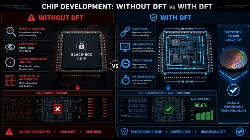
Without DFT infrastructure, the debug team has very limited visibility into the internal state of the chip. Engineers must rely on software tests, external observations, and educated guesses to find the source of the problem. Days quickly turn into weeks as they investigate one possibility after another. Eventually, they trace the issue to a timing problem in a specific pipeline stage, something proper test structures could have surfaced far earlier.
Now consider the same design with DFT integrated from the start. Scan chains let engineers capture and observe the state of internal flip-flops, while ATPG (Automatic Test Pattern Generation) patterns deliver high fault coverage and efficient diagnostics. When a defect appears, diagnostic tools narrow it to a small set of likely locations. This cuts debug effort sharply and accelerates root-cause analysis.
This gap in debug efficiency is one of the strongest arguments for Design for Test. Designs without DFT often behave like a black box during silicon validation, which makes fault isolation slow and resource-intensive. DFT changes that. It provides visibility, controllability, and structured test access, so teams find issues faster, improve yield, and move closer to first-time-right silicon.
The benefits of DFT reach across every phase of a chip’s lifecycle, from first silicon bring-up through mass production. The most immediate advantage is speed. Structured test patterns generated by ATPG tools enable fast, automated manufacturing testing and remove much of the manual effort that non-DFT designs demand. In high-volume production, test time translates directly into cost, so a well-built DFT architecture lowers per-unit test expense and improves manufacturing efficiency.
Earlier fault detection is another key advantage. DFT lets teams apply manufacturing tests to early prototypes and catch process-related defects before they spread across a larger batch. This matters even more at advanced nodes, such as 5nm, 3nm, and below, where manufacturing variation is tighter and defect mechanisms are more subtle.
Fault coverage is the primary metric by which DFT quality is judged. It measures the percentage of potential manufacturing faults the test suite can detect. Industry-leading DFT implementations routinely reach fault coverage above 98%, which sharply reduces the chance that a defective part ships to a customer. Higher coverage improves production yield, the ratio of good die to total die, and lowers field return rates. Both carry major financial weight at scale.
Perhaps the most strategic benefit is fewer silicon re-spins. With well-planned DFT architecture, post-silicon debug cycles get shorter, root causes surface faster, and teams can tell a design bug apart from a manufacturing defect with confidence. Fewer re-spins mean faster time-to-market, which in competitive semiconductor segments can decide whether you win a design or lose it to a rival.
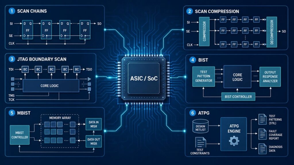
Modern Design for Test relies on a toolbox of complementary techniques. Here are the core methods you will encounter in nearly every ASIC and SoC flow.
Scan chains form the backbone of almost every DFT strategy in modern semiconductor design. In a scan-enabled design, flip-flops across the logic connect into long serial shift registers called scan chains. During test mode, test patterns shift into these chains, a clock captures the circuit’s response, and the resulting data shifts out for comparison against expected values. This approach gives high visibility into internal logic states and detects manufacturing defects efficiently, all while adding relatively little area overhead.
As SoCs grow in complexity, scan chains can hold hundreds of thousands, or even millions, of flip-flops. That creates real challenges for test time and test data volume. Scan compression solves this by using on-chip compression and decompression logic to shrink the test data that must be stored and transferred. By cutting test data volume while keeping fault coverage high, scan compression reduces test time and ATE (Automatic Test Equipment) memory requirements in large SoCs.
Boundary scan, defined by the IEEE 1149.1 standard and widely known as JTAG, extends testability beyond the chip to the board and system level. JTAG infrastructure lets engineers verify chip-to-chip interconnects, access internal debug registers, and perform in-system programming without removing components from a circuit board. Thanks to its versatility and broad adoption, JTAG is now a standard feature in many ASICs, SoCs, FPGAs, and embedded systems.
Built-In Self-Test (BIST) places test generation and response analysis logic directly inside the chip, so specific blocks can test themselves without relying entirely on external equipment. This is especially valuable for complex designs that need fast, repeatable testing.
One of the most widely used forms of BIST is Memory Built-In Self-Test (MBIST). Modern SoCs often devote a large share of silicon area to embedded memories such as SRAMs, ROMs, and register files. MBIST provides an automated, reliable way to detect memory-related defects during manufacturing, and it can also run at system startup or in the field to improve long-term reliability.
Automatic Test Pattern Generation (ATPG) is the software-driven process that creates test patterns targeting specific fault models in a design. Common fault models include stuck-at faults, transition delay faults, path delay faults, and cell-aware faults. ATPG tools analyze the gate-level netlist and automatically generate optimized test vectors that maximize fault coverage while keeping test time and test data volume low.
In modern DFT flows, ATPG plays a central role in high-quality manufacturing tests. The generated patterns are applied through scan chains and other DFT structures, so engineers can identify defects efficiently and ensure that only working devices reach customers. High fault coverage from ATPG directly improves product quality, raises yield, and builds confidence in first-time-right silicon.
Even with mature tools, Design for Test brings challenges that grow at advanced process nodes. Understanding them early helps you plan a stronger test architecture.
As SoC complexity grows, comprehensive test coverage gets harder to achieve. Modern AI accelerators, HPC processors, and advanced SoCs integrate many heterogeneous IP blocks, each with its own clock domains, power domains, and communication interfaces. Controlling and observing all of these blocks through a unified test architecture takes careful planning and close collaboration among design, verification, physical design, and DFT teams.
Power consumption during testing has become a major challenge at advanced nodes. During scan shift, many flip-flops can switch at once, creating current surges well above normal operation. Excessive switching can cause false failures, reliability concerns, or even damage to the device under test. To manage this, modern DFT methodologies use low-power scan techniques such as scan segmentation, clock gating, and switching-activity control to cut test power while preserving fault coverage.
DFT structures such as scan chains, compression logic, and test access networks add routing and fanout to the design. These additions can affect critical timing paths and increase physical implementation complexity. As a result, you must coordinate DFT insertion carefully with physical design and timing sign-off, so testability gains do not hurt performance, power, or area goals.
Balancing fault coverage, test time, and manufacturing cost is another significant challenge. Higher fault coverage usually needs more test patterns, which can raise tester memory use and overall test duration. Semiconductor companies must optimize their DFT strategy to hit quality targets while controlling ATE costs and production test expenses. This often calls for experienced DFT engineers who understand both the technical requirements and the manufacturing economics.
The following Design for Test best practices help teams reach higher fault coverage, shorter debug cycles, and fewer re-spins.
The most effective DFT strategy starts during the architecture phase. Define DFT requirements before RTL development begins, so the team can make informed decisions about scan chain architecture, BIST implementation, JTAG infrastructure, and test access mechanisms. Planning DFT early reduces implementation complexity and avoids costly redesign later. Organizations that treat DFT as an architectural requirement, rather than a post-design activity, typically achieve higher fault coverage, shorter debug cycles, and lower re-spin rates.
Successful DFT depends on close collaboration among design, verification, physical design, and DFT teams. Test logic must be verified as thoroughly as functional logic. A complete DFT verification strategy should include scan chain connectivity checks, ATPG validation, MBIST verification, and JTAG access testing. Confirming that DFT structures work correctly before tapeout helps eliminate test-related issues that could slow silicon bring-up and production readiness.
Coverage-driven DFT methodologies give you a structured, measurable approach to test quality. Define fault coverage goals early and track progress throughout the project, so the team can spot gaps before tapeout. Monitoring coverage metrics supports informed decisions about test architecture and helps ensure the final design meets manufacturing quality objectives.
As SoCs grow in size and complexity, scalable DFT architectures matter more. Reusable test wrappers, scan infrastructures, and MBIST frameworks let IP blocks keep their testability when they move into future projects. A well-documented, reusable DFT architecture lowers development effort, speeds integration, and improves consistency across chip generations. This is especially valuable for organizations that build product families on shared IP and platform architectures.
The demands on Design for Test are evolving fast, driven by three converging trends: the complexity of AI and HPC chip architectures, the difficulty of advanced-node manufacturing, and the strict reliability requirements of automotive-grade semiconductors. AI accelerators built on 3nm and 2nm nodes pack hundreds of billions of transistors and rely on chiplet-based architectures. These designs need test solutions that span die-to-die interconnects, an area where traditional scan-based DFT must be augmented with new protocols and structural test approaches.
AI-assisted ATPG and test generation is an emerging area of strong interest. Machine learning models trained on historical fault and test data can speed up pattern generation, predict coverage gaps, and tune test suites for specific defect distributions. The technology is still maturing, but early implementations already show measurable reductions in pattern count without sacrificing fault coverage.
Automotive-grade reliability standards, especially ISO 26262 for functional safety, impose fault coverage requirements that exceed those of consumer and industrial applications. Random hardware faults, the kind that occur during normal field operation, must be detectable at rates that consumer-grade DFT may not reach. This has driven adoption of on-chip safety monitors, periodic BIST during runtime, and enhanced diagnostic coverage methods built for safety-critical ASIC design.
Design for Test is no longer an optional enhancement for complex ASIC and SoC projects; it is a fundamental requirement for competitive semiconductor engineering. The link between DFT quality and silicon success is direct and measurable. Higher fault coverage produces better yield, faster debug cycles enable shorter re-spin schedules, and structured test infrastructure reduces the cost and risk of moving a chip from design to volume production.
As process nodes keep scaling and architectures grow more heterogeneous, the DFT problem will only get harder. The teams that invest in DFT architecture early, hold rigorous coverage targets throughout the flow, and verify their DFT logic as carefully as their functional logic are the teams that consistently achieve first-time-right silicon.
As semiconductor designs continue to grow in complexity, robust DFT methodologies remain essential for better testability, reliability, and manufacturing quality. Organizations across the industry, including Silicon Patterns, continue to focus on advanced DFT, ATPG, and verification practices to support successful ASIC and SoC development.
Design for Test (DFT) in VLSI is a set of design techniques that add dedicated test structures, such as scan chains and BIST, to a chip. These structures improve the controllability and observability of internal logic, which makes it easier to detect manufacturing defects and achieve high fault coverage.
DFT is important because it enables fast, automated manufacturing testing, earlier fault detection, and shorter debug cycles. Together these reduce silicon re-spins, improve yield, and help teams reach first-time-right silicon, which lowers cost and speeds time-to-market.
Scan chains are the on-chip structures that connect flip-flops into shift registers for test access. ATPG (Automatic Test Pattern Generation) is the software process that creates the test patterns applied through those scan chains to target specific fault models.
Industry-leading DFT implementations routinely achieve fault coverage above 98%. Safety-critical applications governed by standards such as ISO 26262 often target even higher coverage for random hardware faults.

From ASIC architecture to GDSII tape-out — talk to our engineering team today.
Let’s Build Your Next Chip Together.