


Inactive
Simplifying IT
for a complex world.
Platform partnerships
- AWS
- Google Cloud
- Microsoft
- Salesforce
For over a decade, the familiar Fin Field-Effect Transistor (FinFET) architecture served as the essential engine of Moore’s Law, allowing the semiconductor industry to shrink components while controlling leakage current.3 However, in the high-stakes race to build the next generation of processors for AI, high-performance computing (HPC), and mobile devices, the FinFET design has hit an unyielding physical wall.4
To make a FinFET device faster, engineers had to add more parallel fins, which inherently consumed valuable lateral area—a scaling constraint that limited true miniaturization.5 This is why the industry is undergoing a revolutionary architectural shift away from the familiar “nanometer” label (a marketing term for a generation of improvement, not a literal measurement 6) and into the Angstrom Era (2nm is 20 Angstroms).4 This shift is defined by the necessary adoption of the Gate-All-Around FET (GAAFET).5
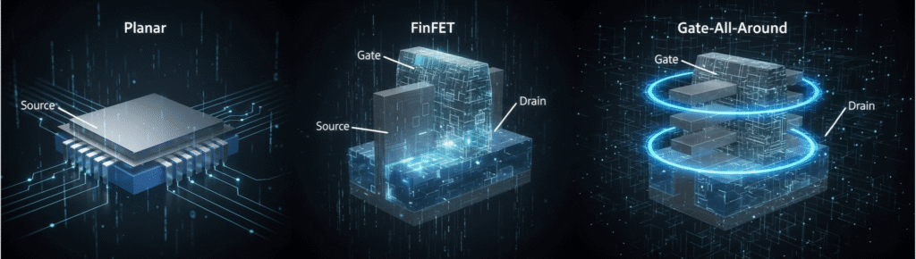
The transition to 2nm process technology is fundamentally a move to the GAAFET structure, which is widely considered the “ultimate CMOS device in terms of electrostatics”.4
Unlike a FinFET, where the gate surrounds only three sides of the channel, a GAAFET completely encloses the entire channel.5 This simple yet profound change allows the gate to regain robust electrostatic control, effectively suppressing leakage currents—a persistent problem as transistors shrink.7
GAAFETs are often implemented using stacked nanosheet or nanowire technology.5 This nanosheet approach offers two crucial benefits over FinFETs:
Leading foundries are implementing their own flavors of this technology: Intel calls its GAAFET implementation RibbonFET (used at its 18A node), and Samsung deployed its variant, the Multi-Bridge Channel FET (MBCFET), at the 3nm node.8
The performance gains at 2nm are not just about the transistor; they are equally reliant on radical re-engineering of the chip’s foundation. This is where the Backside Power Delivery Network (BSPDN) comes into play.9
In traditional chips, power and signal lines compete for space on the top (front side) of the wafer. As density increases, this competition leads to poor power stability and resistance.9 BSPDN resolves this by routing the power supply network through the backside of the wafer, separating it from the signal network.9
This architectural shift offers dramatic gains:
The successful adoption of GAAFETs alongside BSPDN confirms that modern scaling is not just about shrinking; it’s about System-Technology Co-Optimization (STCO)—optimizing devices, interconnects, and packaging simultaneously.8
The 2nm competitive landscape is intense, with major foundries targeting 2025 for mass production of their Angstrom-era nodes.6
| Foundry Node | Architecture | Key Targets (vs. Previous Node) | Production Timeline |
| Intel 18A | RibbonFET (GAA) + PowerVia (BSPDN) | Up to 25% higher frequency (iso-voltage) or 38% power savings (iso-clock) 11 | Enablement H1 2024 (aggressive) 6 |
| TSMC N2 | GAAFET Nanosheet + BSPDN | 10–15% higher performance (iso-power) or 20–30% lower power (iso-performance) 6 | Mass Production H2 2025 6 |
| Samsung 2GAP (SF2) | MBCFET (GAA Variant) + BSPDN | Projected 17% chip size reduction via BSPDN 10 | Production in 2025 6 |
While Intel has set aggressive performance targets, TSMC retains its advantage in reputation for reliable, high-volume manufacturing.8 Regardless of the winner, success relies on deploying these complex technologies, including highly advanced High Numerical Aperture (High-NA) Extreme Ultraviolet (EUV) lithography, which costs nearly $380 million per tool.12
As the industry looks ahead, the roadmap confirms that the future of scaling is decisively vertical.7 The next major architectural leap will be the Complementary FET (CFET), slated for deployment around the A7 (1.8nm) node.7
CFETs solve the last major lateral area constraint of CMOS design by vertically stacking the nFET (negative channel) devices directly on top of the pFET (positive channel) devices.13 This “folding” eliminates the space previously required to separate the two types of transistors, achieving maximum density and paving the way for further gains through three-dimensional integration and advanced packaging techniques.13
The shift to 2nm and beyond is more than a simple node shrink; it is a total architectural overhaul—a “sum of several ‘Aha!’ moments”—that ensures silicon can continue to power the escalating demands of the digital world for years to come.15
Navigating the complexities of GAAFET, BSPDN, and CFET implementation requires specialized expertise. Silicon Patterns offers advanced Silicon Engineering services covering the full design and development lifecycle, including SoC development, prototyping, IC testing, and board design.
Specializing in comprehensive chip design, the company delivers cutting-edge semiconductor solutions and custom chip designs tailored to unique needs. With a focus on client success, Silicon Patterns empowers companies to navigate challenges in AI, IoT, and connected devices, ensuring faster time to market and cost efficiency. Learn how to unlock your business potential and leverage cutting-edge technology.

From ASIC architecture to GDSII tape-out — talk to our engineering team today.
Let’s Build Your Next Chip Together.