


Inactive
Simplifying IT
for a complex world.
Platform partnerships
- AWS
- Google Cloud
- Microsoft
- Salesforce
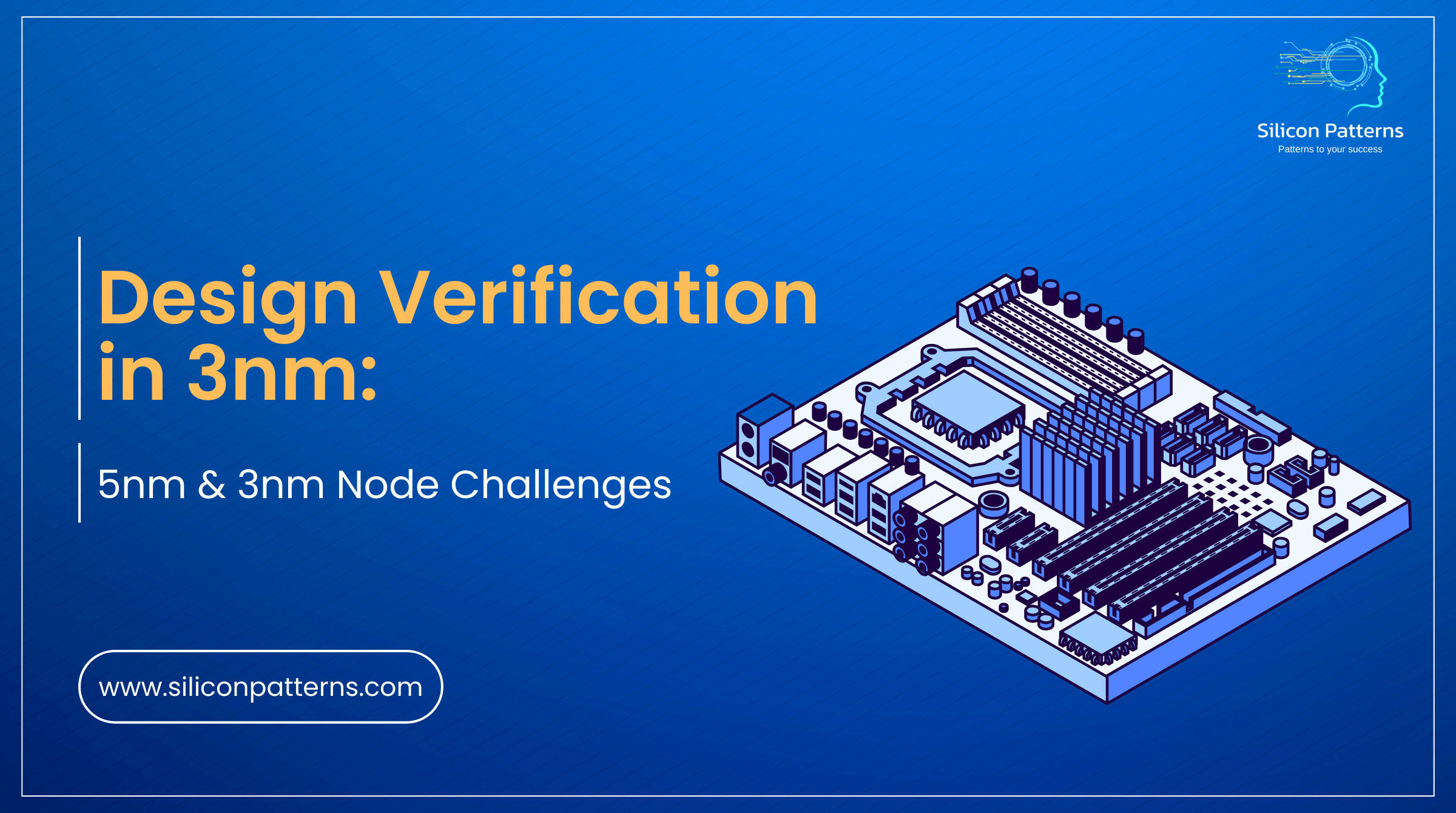
Design verification in 3nm has become one of the most critical stages in advanced semiconductor development. As the industry transitions from 5nm to 3nm node designs, engineers face growing complexity, tighter margins, and increased variability. These advanced nodes demand stronger verification strategies to ensure performance, power efficiency, and first-silicon success.

At 5nm and 3nm, transistor density increases dramatically. Modern SoCs integrate billions of transistors, multiple IP blocks, AI accelerators, high-speed interfaces, and heterogeneous computing architectures.
Verification environments must scale accordingly. Functional verification, formal verification, and emulation need to handle massive state spaces efficiently.
To manage such complexity, companies often rely on advanced verification services like those offered by Silicon Patterns Design Verification Services to ensure robust validation across design stages.
Power efficiency is a primary driver at advanced nodes. However, aggressive power optimization techniques such as dynamic voltage scaling (DVS), power gating, and multi-voltage domains increase verification complexity.
In 3nm designs, even minor voltage fluctuations can cause functional failures. Verification teams must incorporate power-aware methodologies early in the design cycle.
As feature sizes shrink, process variability becomes a dominant issue. Random dopant fluctuations, line-edge roughness, and variability in FinFET and GAA (Gate-All-Around) structures impact circuit behavior.
Design verification in 3nm technology must include advanced timing signoff, multi-corner analysis, and statistical verification approaches to ensure first-silicon success.
For deeper insights into process challenges at advanced nodes, refer to industry analysis from resources like SEMI (https://www.semi.org), which tracks semiconductor technology trends.
With metal pitches shrinking and routing congestion increasing, signal integrity issues are more pronounced at 5nm and 3nm.
Verification teams must incorporate advanced extraction models and SI-aware simulations to avoid late-stage failures.
Design-for-Test (DFT) implementation becomes increasingly complicated at smaller nodes.
Verification must ensure complete coverage without compromising power or performance. This requires tight collaboration between DFT and verification teams.
Many 3nm designs adopt chiplet architectures and advanced packaging techniques such as 2.5D and 3D stacking.
Traditional verification flows must evolve to handle system-level validation across multiple dies.
The sheer size of 3nm SoCs pushes simulation and emulation tools to their limits.
To address this, teams are adopting:
Efficient methodologies are essential to maintain time-to-market competitiveness.
Reliability concerns increase significantly at 5nm and 3nm nodes.
Verification must account for long-term degradation and mission-mode reliability to ensure product longevity.
To overcome these challenges, organizations should adopt:
Strategic partnerships with experienced verification providers can significantly reduce risk and improve first-pass silicon success rates.
The transition to 5nm and 3nm nodes has redefined semiconductor innovation—but it has also elevated verification complexity to unprecedented levels. From power integrity and variability to signal integrity and advanced packaging, every aspect of chip design demands meticulous validation.
Design verification in 3nm technology is no longer just a functional check—it is a multi-dimensional challenge requiring advanced tools, scalable methodologies, and expert execution.
At Silicon Patterns, we specialize in advanced-node verification solutions tailored for 5nm and 3nm designs. Our expertise in functional verification, formal verification, DFT validation, and power-aware methodologies ensures high-quality silicon with reduced time-to-market.
Partner with Silicon Patterns to confidently navigate the complexities of next-generation semiconductor design and achieve first-pass silicon success.

From ASIC architecture to GDSII tape-out — talk to our engineering team today.
Let’s Build Your Next Chip Together.